


Nand vs v nand top
Nand vs v nand top, Schematic diagrams of 3D NAND architecture a vertical gate and b Download Scientific Diagram top
$0 today, followed by 3 monthly payments of $12.00, interest free. Read More
Nand vs v nand top
Schematic diagrams of 3D NAND architecture a vertical gate and b Download Scientific Diagram
96 layer 3D NAND Flash Transcend Information Inc
3D NAND Flash memory Making HDDs obsolete in a data centric economy
3D NAND Structure 3D Metrology Illuminating Semiconductors
3D NAND Race Faces Huge Tech And Cost Challenges
Figure 2 from 2D vs 3D NAND technology Reliability benchmark Semantic Scholar
globalhousenews.com
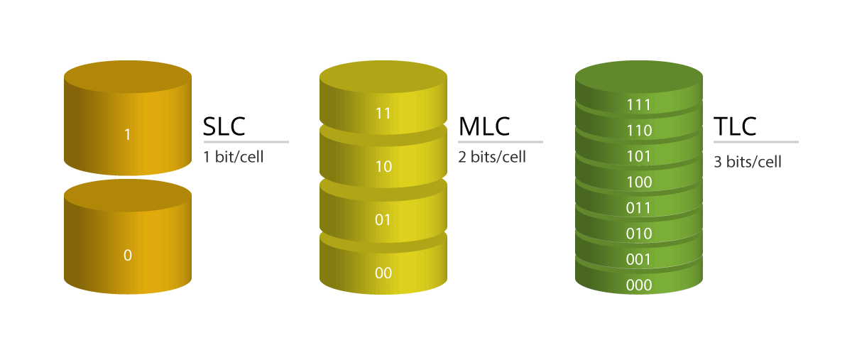
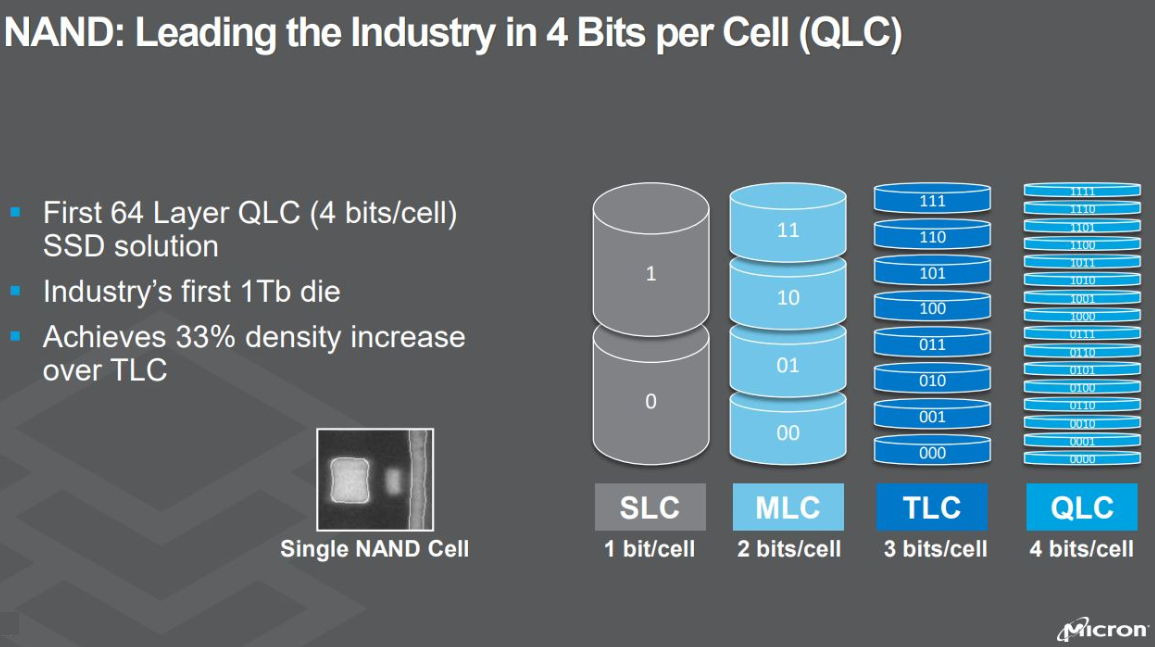
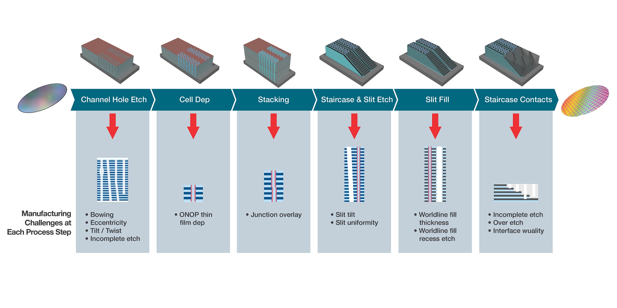
Product Item: Nand vs v nand top2D NAND vs 3D NAND vs V NAND How are they different top, Vertical NAND with and without TSV a closer look top, Difference between SLC MLC TLC and 3D NAND in USB flash drives SSDs and memory cards Kingston Technology top, Why More Companies Are Choosing NAND Flash Memory Today The ICT Trends top, 3D NAND How It Works Samsung SSD 850 Pro 128GB 256GB 1TB Review Enter the 3D Era top, Samsung says 256 layer V NAND memory possible with double stack technology Yonhap News Agency top, NAND Technology Development at SK hynix Reaching New Heights SK hynix Newsroom top, Samsung s V NAND Hitting the Reset Button on NAND Scaling top, Comparison of 3D NAND structures between BiCS Toshiba and VSAT Our. Download Scientific Diagram top, Samsung 850 EVO SSD With 3rd Gen 48 Layer V NAND Performance Comparison The SSD Review top, What Is 3D NAND Types Pros Cons ESF top, Intel promises 10TB SSDs thanks to 3D Vertical NAND flash memory KitGuru top, Flashback The Evolution of NAND Flash Technology SK hynix Newsroom top, What is 3D NAND flash Definition from TechTarget top, 41KB 2001 null null null 3 null null 3 1 2003 null I4 DzaDdUaNQPM top, News Understand the difference between different grades of SSD Chips of NAND Flash SLC MLC TLC QLC top, 2D NAND vs. 3D NAND Pure Storage Blog top, NVMe vs. NAND Technologies Understanding the Basics NVM Express top, Samsung V NAND A Landmark of the Hyperscale AI Era Samsung Semiconductor EMEA top, 3D NAND vs 2D NAND Challenges in Industrial Applications top, How 3D NAND Can Continue Gigabytes Scaling Enhance Applications SD Association top, 3D NAND Flash Wars Begin top, 3D NAND vs 2D NAND What s the Difference in NAND Flash Memory top, Schematic diagrams of 3D NAND architecture a vertical gate and b Download Scientific Diagram top, 96 layer 3D NAND Flash Transcend Information Inc top, 3D NAND Flash memory Making HDDs obsolete in a data centric economy top, 3D NAND Structure 3D Metrology Illuminating Semiconductors top, 3D NAND Race Faces Huge Tech And Cost Challenges top, Figure 2 from 2D vs 3D NAND technology Reliability benchmark Semantic Scholar top, 232 layer NAND Micron Technology Inc top, Inhibited Channel Potential of 3D NAND Flash Memory String According to Transient Time top, 3D NAND Flash Memory Market Industry Analysis and Forecast top, What is 2024 3d nand top, 2D NAND vs 3D NAND vs V NAND How are they different top, Tech Brief Memory Grows Up with 3D NAND top.
-
Next Day Delivery by DPD
Find out more
Order by 9pm (excludes Public holidays)
$11.99
-
Express Delivery - 48 Hours
Find out more
Order by 9pm (excludes Public holidays)
$9.99
-
Standard Delivery $6.99 Find out more
Delivered within 3 - 7 days (excludes Public holidays).
-
Store Delivery $6.99 Find out more
Delivered to your chosen store within 3-7 days
Spend over $400 (excluding delivery charge) to get a $20 voucher to spend in-store -
International Delivery Find out more
International Delivery is available for this product. The cost and delivery time depend on the country.
You can now return your online order in a few easy steps. Select your preferred tracked returns service. We have print at home, paperless and collection options available.
You have 28 days to return your order from the date it’s delivered. Exclusions apply.
View our full Returns and Exchanges information.
Our extended Christmas returns policy runs from 28th October until 5th January 2025, all items purchased online during this time can be returned for a full refund.